Applications / Semiconductor
Autofocus in optical inspection: speed-resolution tradeoffs in piezo-driven lens stages
How piezoelectric actuators enable the autofocus performance that high-throughput optical inspection demands
Autofocus in Optical Inspection: Speed-Resolution Tradeoffs in Piezo-Driven Lens Stages
Optical inspection tools for semiconductor manufacturing must image wafer surfaces at nanometer-scale resolution while maintaining throughput of tens to hundreds of wafers per hour. The autofocus system, which keeps the imaging optics precisely focused on the wafer surface as it scans, is a critical subsystem that directly limits both image quality and throughput. The autofocus actuator must respond to surface height variations of micrometers within milliseconds, holding focus to within tens of nanometers.
Piezoelectric actuators have become the standard technology for autofocus lens stages in high-performance optical inspection. This article examines the autofocus loop requirements, the physics of the speed-resolution tradeoff, lens mass and inertia effects, integration with through-the-lens (TTL) autofocus sensing, and the performance numbers that current systems achieve. For the wafer stage positioning context in which these autofocus systems operate, see the companion article on sub-nm wafer stage positioning.
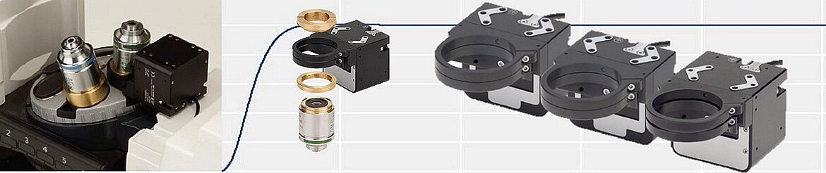
Image: Physik Instrumente (PI)
The Autofocus Problem
A high-NA (numerical aperture) microscope objective has a depth of focus (DOF) determined by the Rayleigh criterion:
DOF = +/- (n * lambda) / (2 * NA^2)
For a typical inspection objective with NA = 0.9, wavelength lambda = 365 nm (i-line), and n = 1 (air):
DOF = +/- (1 * 365) / (2 * 0.81) = +/- 225 nm
For a deep UV objective at 266 nm with NA = 0.95:
DOF = +/- (1 * 266) / (2 * 0.9025) = +/- 147 nm
The total DOF is approximately 300 to 450 nm, depending on the optical configuration. The autofocus system must maintain the lens-to-wafer distance within this range, which means the autofocus error budget is roughly +/- 100 to 200 nm (allowing margin for other focus contributors such as lens aberration and wafer tilt).
This is the fundamental challenge: the wafer surface is not flat. It has topography from process steps (typically 0.1 to 10 micrometers of height variation), wafer bow and warp (up to 200 micrometers across 300 mm), and local flatness variations from the chuck (0.1 to 1 micrometer). As the wafer scans under the objective, the surface height changes continuously, and the autofocus must track these changes in real time.
Autofocus Loop Architecture
A modern optical inspection autofocus system consists of four main components:
1. Focus Sensor
The focus sensor measures the distance between the objective lens and the wafer surface. Several sensing technologies are used:
Through-the-lens (TTL) autofocus: A separate autofocus beam (typically an LED or laser at a wavelength outside the imaging band) is projected through the objective onto the wafer and reflected back to a position-sensitive detector. The detector measures the defocus signal (the displacement of the reflected beam from its in-focus position). TTL autofocus automatically compensates for any relative motion between the objective and the sensor because both share the same optical path.
Resolution: 5 to 50 nm. Bandwidth: limited by detector integration time and electronics, typically 10 to 100 kHz. The TTL approach is the most accurate because it measures the actual optical focus error, not a mechanical proxy.
Chromatic confocal sensing: A broadband light source is focused through a chromatic lens (with high axial chromatic aberration) onto the wafer. Different wavelengths focus at different heights. A spectrometer analyzes the reflected spectrum to determine the surface height. Resolution: 10 to 100 nm. Bandwidth: limited by spectrometer frame rate, typically 1 to 70 kHz.
Capacitive or air gauge sensing: A non-optical sensor measures the distance between a reference surface (attached to the objective housing) and the wafer. Resolution: 1 to 10 nm. Bandwidth: 10 to 100 kHz. These sensors measure mechanical distance rather than optical focus and therefore do not automatically compensate for thermal drift of the objective focal length or changes in the optical path.
2. Controller
The autofocus controller processes the focus sensor signal and generates a command to the actuator. The controller must:
- Run at a sample rate of 10 to 100 kHz (10x to 100x the required autofocus bandwidth).
- Implement a servo loop with proportional-integral-derivative (PID) or more advanced control (feedforward, model-based, or learning-based).
- Handle sensor noise without amplifying it into actuator jitter.
- Provide feedforward compensation for known wafer topography (from a wafer map or a look-ahead sensor).
3. Actuator (Piezo-Driven Lens Stage)
The actuator moves the objective lens (or the entire lens assembly) along the optical axis (Z) to maintain focus. This is the component where motor selection has the most direct impact on performance.
4. Mechanical Structure
The objective housing, flexure stage, and mounting structure must be stiff enough to maintain alignment (decenter and tilt below specification) while allowing the required Z travel. The structural resonance must be high enough to support the control bandwidth.
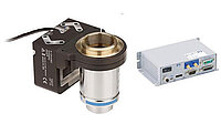
Image: Physik Instrumente (PI)
Speed-Resolution Tradeoff: The Core Engineering Challenge
The autofocus system faces a fundamental tradeoff: faster response requires wider control bandwidth, which amplifies sensor noise and actuator noise, degrading focus resolution. Slower response reduces noise but cannot track rapid surface height changes, causing focus error during scanning.
Quantifying the Tradeoff
Consider a wafer scanning at velocity v under an objective. A surface height step of amplitude h over a lateral distance d creates a height rate of change:
dz/dt = v * h / d
For a scanning velocity of 100 mm/s, a 1 micrometer height step over 10 micrometers of lateral distance:
dz/dt = 0.1 * 1 / 0.01 = 10 mm/s
The autofocus must slew at 10 mm/s to track this step. For a piezo stack with 50 micrometer range, slewing the full range takes 50/10000 = 5 ms. This is a modest requirement for a piezo actuator.
However, the more demanding case is a sinusoidal surface variation (such as wafer bow or periodic process topography). If the wafer has a sinusoidal height variation with amplitude A and spatial period P, the required autofocus tracking bandwidth is:
f_AF = v / P
For v = 200 mm/s and P = 0.5 mm (a fast spatial frequency from a process pattern):
f_AF = 200 / 0.5 = 400 Hz
The autofocus bandwidth must exceed 400 Hz to track this surface variation. At 400 Hz bandwidth, the focus error from a sinusoidal surface of amplitude A is approximately:
e_focus = A * (f_surface / f_AF)^2 (for frequencies above f_AF) e_focus = A * sqrt(1 + (f_surface / f_AF)^2) (near f_AF)
For surface amplitudes of 500 nm at 400 Hz, the residual error at the control bandwidth crossover is approximately 500 * sqrt(2) * (1/1) = 700 nm for a simple integrator, or much less with a well-designed servo. A second-order servo with 400 Hz bandwidth and 0.7 damping ratio achieves less than 100 nm tracking error for a 500 nm amplitude sinusoidal surface at 400 Hz.
Noise Amplification at High Bandwidth
The penalty for high bandwidth is noise amplification. The focus sensor has a noise floor, typically 2 to 10 nm RMS for a TTL sensor at 10 kHz measurement rate. The servo loop amplifies high-frequency sensor noise by the closed-loop sensitivity function. For a well-designed servo at bandwidth f_AF, the noise amplification peak is typically 3 to 6 dB (1.4x to 2x) near the bandwidth frequency.
Additionally, the piezo amplifier has voltage noise that translates to position noise. A typical low-noise piezo amplifier has 100 to 300 microvolt RMS noise in a 10 kHz bandwidth. For a piezo stack with a sensitivity of 1 micrometer per volt, this is 0.1 to 0.3 nm RMS, which is negligible. But for wider bandwidth (higher amplifier bandwidth), the noise increases as the square root of bandwidth.
The total autofocus noise at bandwidth f_AF can be estimated as:
sigma_AF = sqrt(sigma_sensor^2 * G_CL^2 + sigma_amp^2 * G_amp^2)
where G_CL is the closed-loop noise gain (approximately 1 to 2 near crossover) and G_amp is the amplifier noise gain.
For a 1 kHz bandwidth servo with a 5 nm RMS sensor noise floor:
sigma_AF = sqrt((5)^2 * (1.5)^2 + (0.2)^2 * (1)^2) = sqrt(56.3 + 0.04) = 7.5 nm RMS
For a 3 kHz bandwidth servo (wider bandwidth means higher sensor noise due to shorter integration time):
Sensor noise at 3 kHz measurement rate: 5 * sqrt(3) = 8.7 nm RMS (noise scales as sqrt of bandwidth) sigma_AF = sqrt((8.7)^2 * (2)^2 + (0.35)^2 * (1)^2) = sqrt(302 + 0.12) = 17.4 nm RMS
Tripling the bandwidth from 1 kHz to 3 kHz more than doubled the autofocus noise, from 7.5 nm to 17.4 nm RMS. This is the speed-resolution tradeoff in quantitative terms.
Optimal Bandwidth Selection
The optimal autofocus bandwidth minimizes the total focus error, which is the sum of the tracking error (decreases with bandwidth) and the noise error (increases with bandwidth).
For a specific wafer and scan speed, the tracking error power spectral density falls off as 1/f^2 above the bandwidth. The noise error power spectral density increases as f^(1/2) (sensor noise scaling) above the bandwidth. The optimal bandwidth is where the marginal reduction in tracking error equals the marginal increase in noise error.
In practice, this optimal bandwidth ranges from 200 Hz (for smooth wafers at low scan speeds) to 3 kHz (for rough wafers at high scan speeds). Most inspection tools implement adaptive bandwidth control, adjusting the servo parameters based on the measured surface roughness and scan velocity.
Lens Mass and Inertia Effects
The objective lens assembly is the payload that the autofocus actuator must move. Its mass and inertia directly determine the achievable bandwidth and settling time.
Mass Budget
A typical high-NA inspection objective (0.9 NA, 365 nm) has a mass of 200 to 800 g, depending on the design. Larger objectives with more elements (for wider field or lower aberration) are heavier. The lens housing and mounting hardware add 100 to 300 g. The total moving mass for the autofocus stage is typically 300 g to 1.2 kg.
Resonance Frequency and Bandwidth
For a piezo stack actuator with stiffness k_piezo driving a mass m through a flexure with stiffness k_flexure, the first resonant frequency is:
f_res = (1 / (2 * pi)) * sqrt((k_piezo + k_flexure) / m)
The closed-loop bandwidth of the autofocus servo is limited to approximately 1/3 to 1/2 of this resonant frequency (to maintain adequate phase margin).
For a typical system:
- Piezo stiffness: 50 to 200 N/micrometer (a multilayer stack)
- Flexure stiffness: 1 to 10 N/micrometer (designed to be much less than the piezo, so the piezo determines the motion)
- Effective stiffness: limited by the flexure and preload arrangement; typically 10 to 50 N/micrometer at the output
- Moving mass: 500 g
f_res = (1 / (2 * pi)) * sqrt(20 * 10^6 / 0.5) = 1007 Hz
Achievable bandwidth: 300 to 500 Hz.
To double the bandwidth to 1 kHz, either the stiffness must quadruple (to 80 N/micrometer at the output) or the mass must be quartered (to 125 g). Since the objective lens mass is not easily reduced (it is determined by optical design), the design effort focuses on increasing stage stiffness.
Stiffness Design Strategies
Preloaded piezo stacks: Using opposing piezo stacks in a push-pull configuration increases the effective stiffness by 2x compared to a single stack (one stack pushes while the other acts as a stiff spring). The push-pull configuration also linearizes the response and eliminates the need for a return spring.
Parallel flexure design: Using multiple flexure blades in parallel increases the lateral stiffness (which prevents the lens from tilting during Z motion) without affecting the Z-axis stiffness (which is set by the piezo).
Direct-drive coupling: Eliminating any lever or amplifier mechanism between the piezo and the lens ensures that the full piezo stiffness is available at the output. Lever mechanisms multiply travel at the expense of stiffness (stiffness decreases as the square of the lever ratio).
Lightweight lens support: Using the minimum possible material for the lens housing and flexure stage. Materials with high stiffness-to-density ratio (silicon carbide, beryllium, carbon fiber composite) enable lighter stages. Beryllium, with a modulus/density ratio 6x higher than aluminum, is used in the highest-performance autofocus stages, though its toxicity makes machining expensive.
Worked Example: Autofocus Stage for a 266 nm Inspection Tool
Requirements:
- Autofocus bandwidth: 1 kHz
- Z travel range: +/- 25 micrometers (50 micrometers total)
- Focus resolution: 10 nm RMS
- Objective mass: 400 g
- Total moving mass (including lens housing and flexure): 600 g
Actuator selection:
Required resonant frequency: 1 kHz * 3 = 3 kHz (for adequate phase margin) Required stiffness: k = m * (2 * pi * f_res)^2 = 0.6 * (2 * pi * 3000)^2 = 213 * 10^6 N/m = 213 N/micrometer
This is a high stiffness requirement. A single multilayer piezo stack of 10 x 10 x 36 mm has a stiffness of approximately 200 N/micrometer and a free stroke of approximately 40 micrometers at 150 V. Three such stacks in a parallel kinematic arrangement would provide more than adequate stiffness and travel.
However, the flexure compliance reduces the effective output stiffness. If the flexure has a Z-axis stiffness of 50 N/micrometer, the combined stiffness is:
1/k_total = 1/k_piezo + 1/k_flexure = 1/200 + 1/50 = 0.005 + 0.02 = 0.025 k_total = 40 N/micrometer
This gives a resonant frequency of only:
f_res = (1 / (2 * pi)) * sqrt(40 * 10^6 / 0.6) = 1300 Hz
Achievable bandwidth: approximately 430 Hz. This is well below the 1 kHz target.
Solution: Redesign the flexure to increase its Z-axis stiffness. Using thicker flexure blades and shorter blade length increases stiffness at the expense of travel range (the flexure must still accommodate +/- 25 micrometers). A stiffness of 200 N/micrometer in the flexure, combined with the 200 N/micrometer piezo, gives:
1/k_total = 1/200 + 1/200 = 0.01 k_total = 100 N/micrometer
f_res = (1 / (2 * pi)) * sqrt(100 * 10^6 / 0.6) = 2056 Hz
Achievable bandwidth: approximately 700 Hz. Still below 1 kHz.
To reach 1 kHz bandwidth, reduce the moving mass. Replacing the aluminum lens housing with beryllium (density: 1.85 g/cm^3 vs. 2.7 g/cm^3 for aluminum; modulus: 287 GPa vs. 69 GPa for aluminum) reduces the housing mass from 200 g to 80 g. New total moving mass: 480 g.
f_res = (1 / (2 * pi)) * sqrt(100 * 10^6 / 0.48) = 2298 Hz
Achievable bandwidth: approximately 770 Hz to 1.1 kHz (depending on controller design). The 1 kHz target is now achievable with an advanced controller (e.g., model-based feedforward plus PID feedback).
This worked example illustrates why autofocus stage design is a system-level optimization involving the actuator, flexure, lens housing material, and controller. No single component change achieves the required performance alone.
TTL Autofocus Integration
Through-the-lens autofocus is the preferred sensing method for high-accuracy optical inspection because it measures the true optical focus error, not a mechanical proxy.
TTL Sensor Architecture
A TTL autofocus sensor projects a structured illumination pattern (typically a line or grid) through the objective onto the wafer surface. The reflected pattern is captured by a detector (a linear CCD/CMOS array or a position-sensitive detector, PSD) located at a conjugate plane. When the wafer is in focus, the reflected pattern is centered on the detector. When the wafer is above or below focus, the pattern shifts on the detector proportionally to the defocus distance.
The sensitivity of the TTL sensor is:
S = dx_detector / dz_wafer = 2 * NA^2 * M_AF / lambda_AF
where M_AF is the magnification of the autofocus imaging path and lambda_AF is the autofocus wavelength. For NA = 0.9, M_AF = 10, and lambda_AF = 780 nm (near-infrared LED):
S = 2 * 0.81 * 10 / 0.78 = 20.8 micrometers of detector shift per micrometer of defocus
With a detector pixel size of 5 micrometers, a 1 micrometer defocus produces a 20.8 micrometer shift, or approximately 4 pixels. Sub-pixel interpolation achieves 0.01 to 0.1 pixel resolution, translating to 2.4 to 24 nm focus resolution.
Integration Challenges
Wavelength separation: The TTL autofocus beam must not interfere with the imaging beam. This requires wavelength separation using dichroic beam splitters. The autofocus wavelength is typically in the near-infrared (780 to 980 nm) for visible-light inspection tools, or in the visible range for deep UV inspection tools. The dichroic beam splitter must achieve greater than 99% reflection of the autofocus beam and greater than 99% transmission of the imaging beam to avoid ghost images or signal loss.
Latency: The TTL sensor introduces latency (delay) between the focus measurement and the actuator response. The total latency includes detector integration time (10 to 100 microseconds), readout time (1 to 10 microseconds), controller computation time (1 to 10 microseconds), and amplifier response time (1 to 10 microseconds). Total latency of 20 to 100 microseconds is typical.
Latency limits the achievable control bandwidth. A phase delay of 45 degrees at the crossover frequency is the maximum allowable for adequate stability margin. The latency-induced phase delay is:
phi = 360 * f_AF * t_latency (degrees)
For f_AF = 1 kHz and t_latency = 50 microseconds:
phi = 360 * 1000 * 0.00005 = 18 degrees
This 18 degrees of phase delay is acceptable (well within the 45 degree budget). But at 3 kHz bandwidth with 50 microsecond latency:
phi = 360 * 3000 * 0.00005 = 54 degrees
This exceeds the 45 degree budget, requiring either reduced latency (faster sensor and electronics) or reduced bandwidth. This is another manifestation of the speed-resolution tradeoff: higher bandwidth demands faster (and noisier) sensors.
Surface reflectivity variations: Wafer surfaces have varying reflectivity due to thin film interference, patterned features, and material changes. The TTL sensor signal amplitude varies with reflectivity, which can cause gain variations in the autofocus loop. Automatic gain control (AGC) or normalized detection schemes compensate for this, but the compensation introduces additional noise at low signal levels.
Typical Performance Numbers
The following table summarizes autofocus performance for representative optical inspection tools across different technology generations.
| Parameter | Brightfield inspector (i-line) | Brightfield inspector (DUV) | Darkfield inspector | High-speed review SEM |
|---|---|---|---|---|
| Imaging wavelength | 365 nm | 266 nm | 405 or 488 nm | N/A (e-beam) |
| Objective NA | 0.9 | 0.95 | 0.7 to 0.9 | N/A |
| Depth of focus | +/- 225 nm | +/- 147 nm | +/- 250 to 410 nm | N/A |
| AF bandwidth | 500 to 1000 Hz | 1000 to 3000 Hz | 300 to 800 Hz | 100 to 500 Hz |
| AF resolution (RMS) | 10 to 20 nm | 5 to 15 nm | 15 to 30 nm | 20 to 50 nm |
| AF travel range | +/- 25 to 50 um | +/- 10 to 25 um | +/- 25 to 100 um | +/- 50 to 200 um |
| Settling time (to within 20 nm) | 2 to 5 ms | 1 to 3 ms | 3 to 10 ms | 5 to 20 ms |
| Scan speed | 50 to 200 mm/s | 100 to 500 mm/s | 100 to 300 mm/s | 10 to 50 mm/s |
| AF sensor type | TTL (LED) | TTL (laser diode) | TTL or separate | Capacitive or TTL |
| AF actuator | Piezo stack + flexure | Piezo stack + flexure | Piezo stack + flexure | Piezo or voice coil |
| Moving mass | 300 to 800 g | 300 to 600 g | 200 to 500 g | 50 to 200 g |
Several trends are apparent:
-
DUV inspectors require the highest autofocus bandwidth (up to 3 kHz) because their shallower depth of focus demands tighter focus control, and their higher scan speeds create faster surface height variations.
-
The autofocus resolution is consistently 5% to 10% of the depth of focus, leaving adequate margin for other focus error contributors.
-
Piezo stack actuators with flexure stages are the universal choice for the autofocus actuator. Voice coil actuators appear only in SEM review tools, where the lower bandwidth requirement and lighter payload (just a focus sensor, not an objective lens) relax the stiffness and bandwidth demands.
-
Settling time of 1 to 5 ms is standard, determined by the piezo stage bandwidth and the initial defocus magnitude after a step move.
Feedforward Enhancement
Pure feedback autofocus (measuring focus error and correcting it) is limited by the sensor-actuator loop delay. Feedforward autofocus anticipates surface height changes and drives the actuator proactively, before the feedback sensor detects an error.
Look-Ahead Sensing
A separate height sensor, located ahead of the objective along the scan direction, measures the wafer surface height before it arrives under the imaging objective. The time between the look-ahead measurement and the imaging exposure is:
t_lookahead = d_sensor_offset / v_scan
For a sensor offset of 10 mm and a scan velocity of 200 mm/s:
t_lookahead = 10 / 200 = 50 ms
This 50 ms of advance notice is enormous compared to the 1 to 3 ms servo settling time. The feedforward path can pre-position the autofocus actuator to the expected focus position well before the imaging occurs. The feedback loop then corrects only the residual error between the predicted and actual surface height.
With feedforward, the effective autofocus bandwidth can exceed the feedback bandwidth by 3x to 10x, because the feedback loop only needs to correct small residual errors rather than track the full surface topography.
Wafer Map Feedforward
For repeated inspection of the same wafer type, the surface topography map from a previous scan can be stored and used as feedforward data for subsequent scans. This is particularly effective for wafers with regular, repeating topography (such as memory arrays).
The accuracy of map-based feedforward depends on the wafer-to-wafer repeatability of the topography. For well-controlled processes, wafer-to-wafer height variation is 10 to 50 nm RMS, which means the map feedforward reduces the feedback loop's tracking load from micrometers to tens of nanometers.
Piezo Amplifier Considerations
The piezo amplifier drives the actuator and directly affects autofocus performance. Key amplifier specifications include:
Bandwidth: The amplifier must have bandwidth 3x to 10x higher than the autofocus servo bandwidth to avoid introducing significant phase delay. For a 1 kHz autofocus bandwidth, the amplifier needs 3 to 10 kHz bandwidth.
Noise: Amplifier voltage noise translates directly to position noise. For a 10 micrometer/150 V piezo sensitivity (67 nm/V), an amplifier with 200 microvolt RMS noise produces 0.013 nm RMS position noise, which is negligible. However, high-bandwidth amplifiers typically have higher noise than low-bandwidth amplifiers, creating another speed-resolution tradeoff.
Slew rate: The amplifier must deliver enough current to charge the piezo capacitance at the required speed. A piezo stack with 5 microfarads capacitance driven at 50 micrometers amplitude (corresponding to approximately 100 V) at 1 kHz requires a peak current of:
I_peak = C * dV/dt = 5 * 10^-6 * (2 * pi * 1000 * 100) = 3.14 A
The amplifier must deliver 3.14 A peak at 150 V, corresponding to 471 W of instantaneous power. This is a significant power level that requires a purpose-built piezo amplifier (standard laboratory amplifiers are typically limited to 0.5 to 1 A).
Linearity: Amplifier nonlinearity (from output stage distortion) adds harmonic content to the focus position, degrading the effective resolution. Total harmonic distortion (THD) below 0.01% is required for sub-10 nm focus accuracy.
Comparison with Voice Coil Autofocus
Voice coil actuators are the main alternative to piezo for autofocus applications. Their advantages and disadvantages are instructive.
Voice coil advantages: Longer travel range (millimeters vs. tens of micrometers). No hysteresis. Linear force-current relationship. Lower cost for large-displacement applications.
Voice coil disadvantages: Lower stiffness (voice coils are force generators, not displacement generators; they require external springs or servos to provide stiffness). Higher power dissipation (continuous current required to maintain position). Magnetic stray fields (can interfere with SEM or other electron-beam-based tools). Lower bandwidth for a given payload mass (due to lower stiffness).
For a 500 g payload, a voice coil autofocus stage typically achieves 200 to 500 Hz bandwidth (limited by the voice coil's force constant and the required spring stiffness). A piezo stack stage achieves 500 to 2000 Hz bandwidth. This 2x to 4x bandwidth advantage is why piezo dominates in high-performance optical inspection autofocus.
Voice coils are preferred in applications where long travel range is critical and bandwidth requirements are modest: for example, in confocal microscopes where the focus stage scans through the full wafer thickness (775 micrometers for a 300 mm wafer), or in SEM review tools where the autofocus bandwidth is limited by the electron beam scan rate rather than the actuator.
Summary
Autofocus in optical inspection is a system-level problem where the piezoelectric actuator sits at the intersection of competing demands: speed, resolution, travel range, and payload mass. The key engineering tradeoffs are:
-
Bandwidth vs. noise: Higher bandwidth enables faster scanning and tracking of rougher surfaces, but amplifies sensor and actuator noise. The optimal bandwidth depends on the specific wafer topography and scan speed.
-
Stiffness vs. travel: Higher stiffness enables higher bandwidth (for a given mass), but short, stiff flexures limit travel range. The stage designer must balance these constraints against the required focus range.
-
Mass vs. optical performance: Lighter objective lenses enable higher autofocus bandwidth, but optical performance (aberration, field size, NA) generally requires more glass elements and therefore more mass.
-
Feedback vs. feedforward: Pure feedback is simpler but limited in bandwidth. Feedforward (from look-ahead sensors or wafer maps) can dramatically extend the effective tracking bandwidth, but requires additional sensors and computation.
Piezoelectric actuators dominate this application because they provide the unique combination of high stiffness, high bandwidth, nanometer resolution, and compact size needed to focus a heavy objective lens at kilohertz rates. As inspection tools push to shorter wavelengths (EUV actinic inspection at 13.5 nm) and higher throughputs (500+ wph), the demands on autofocus actuators will only intensify, making continued improvement in piezo stage technology essential for the semiconductor industry's roadmap.