Applications / Semiconductor
Sub-nm wafer stage positioning: motor selection for 300mm platforms
How piezoelectric actuators deliver the positioning accuracy that advanced semiconductor inspection demands
Sub-nm Wafer Stage Positioning: Motor Selection for 300mm Platforms
Advanced semiconductor inspection at the 3 nm node and below places extraordinary demands on wafer stage positioning. The stage must move a 300 mm wafer (roughly 125 g of silicon, plus chuck mass) across travel ranges of 300+ mm while holding positional accuracy below 1 nm during measurement. That requirement eliminates most motor technologies and, in practice, leaves piezoelectric drives as the dominant solution for fine positioning.
This article examines why, walking through the positioning budget, vibration constraints, vacuum compatibility, and throughput requirements that define motor selection for 300 mm wafer stages.
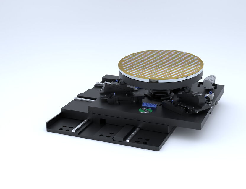
Image: SmarAct GmbH
The Positioning Budget at Advanced Nodes
At the 3 nm logic node, overlay requirements for multi-patterning sit around 1.5 nm (3-sigma). The total overlay budget is split among contributions from the lithography tool, the reticle stage, the wafer stage, metrology, and process-induced distortions. The wafer stage typically receives an allocation of 0.3 to 0.5 nm of that total budget.
For inspection tools (rather than lithography), the accuracy requirements are slightly different but no less demanding. A scanning electron microscope (SEM) based defect review tool operating at 50,000x magnification with a 2 nm pixel size needs stage positioning repeatability below 1 nm. At this magnification, a 1 nm stage error displaces the image by half a pixel, directly degrading measurement accuracy.
The positioning budget breaks down into several components:
- Following error during scanning: The stage must track a commanded trajectory (typically a raster scan) with error below 0.5 nm RMS.
- In-position stability: Once the stage stops for a measurement, it must hold position to within 0.2 to 0.5 nm peak-to-peak over the measurement integration time (typically 10 to 100 ms).
- Bidirectional repeatability: When the stage returns to a previously visited location, it must land within 0.5 nm of its prior position.
These numbers are not theoretical. They are achievable with current piezoelectric stage technology but impossible with conventional electromagnetic motors alone. The closed-loop control architecture used to track these targets is as important as the actuator itself.
Coarse-Fine Architecture
No single motor technology efficiently covers both the 300+ mm travel range and the sub-nm accuracy requirement. The standard solution is a coarse-fine stage architecture.
The coarse stage provides long-range travel (300 to 450 mm in X and Y) with accuracy on the order of 100 nm. This stage uses linear motors, either iron-core or ironless, depending on the force requirements and magnetic interference constraints. The coarse stage carries the wafer chuck and the fine stage assembly.
The fine stage sits atop the coarse stage and provides short-range correction (typically 50 to 200 micrometers of travel) with sub-nm resolution. This is where piezoelectric actuators dominate. The fine stage accepts the coarse stage's positioning error as its input disturbance and drives it to zero using high-bandwidth feedback.
The separation of these roles is critical. A coarse linear motor optimized for speed over 300 mm of travel will generate vibrations in the tens of nanometers range. The fine piezo stage must reject these disturbances with bandwidth high enough to keep the net error below 1 nm.
Why Not Just Use a Better Linear Motor?
A question that arises frequently: can you build a linear motor accurate enough to avoid the fine stage entirely? In principle, yes, for micron-level accuracy. In practice, no, for sub-nm work. The reasons are fundamental.
Linear motors generate force through interaction between permanent magnets and coils. Cogging forces from iron-core motors introduce periodic disturbances at spatial frequencies related to the magnet pitch (typically 20 to 40 mm). Even ironless (air-bearing) linear motors exhibit force ripple from commutation errors, amplifier noise, and cable disturbances.
The best linear motors achieve force ripple on the order of 0.01% to 0.1% of peak force. For a stage requiring 50 N of continuous force, that translates to 5 to 50 mN of force disturbance. Acting on a 5 kg stage mass, 5 mN produces an acceleration of 1 mm/s^2. Integrated over even a millisecond, that generates position disturbances well above 1 nm.
Piezoelectric actuators, by contrast, generate force through solid-state deformation of a ceramic crystal. There is no cogging, no commutation ripple, and no magnetic field. The dominant noise source is the voltage amplifier, and modern low-noise piezo amplifiers achieve noise floors below 100 microvolts RMS, corresponding to displacement noise below 0.01 nm for a typical stack actuator.
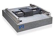
Image: Physik Instrumente (PI)
Vibration Budget and Its Implications
The vibration budget for a sub-nm wafer stage encompasses every source of mechanical disturbance that can degrade positioning accuracy. Understanding and controlling these sources is the core challenge of stage design.
Floor Vibration
Semiconductor fabs are built on massive concrete slabs designed to minimize floor vibration. Typical fab floor vibration specifications call for velocity amplitudes below 3 micrometers/second in the 1 to 100 Hz band (approximately VC-D to VC-E criteria). Converting to displacement, at 10 Hz this corresponds to about 50 nm peak. At 100 Hz, about 5 nm peak.
The tool frame and its vibration isolation system attenuate floor vibration before it reaches the stage. Active pneumatic isolators with feedback control achieve 20 to 40 dB of attenuation above their natural frequency (typically 0.5 to 2 Hz). This reduces 50 nm of floor vibration at 10 Hz to roughly 0.5 to 5 nm at the stage.
A piezo fine stage with 1 kHz bandwidth can further attenuate these disturbances by 40 dB at 10 Hz (assuming second-order rejection), bringing the contribution below 0.05 nm. This layered approach is why the fine stage bandwidth matters: it multiplies the effectiveness of every upstream isolation measure.
Acoustic Excitation
Airborne acoustic noise in a fab cleanroom typically runs 60 to 70 dBA. At frequencies below 200 Hz, acoustic pressure can couple into the stage through the tool frame, generating force disturbances on the order of 0.1 to 1 mN. For inspection tools that operate in ambient air (rather than vacuum), acoustic coupling to the wafer surface itself can induce vibrations of 0.1 to 1 nm.
Tools that operate in vacuum naturally eliminate this acoustic coupling path, which is one reason SEM-based inspection tools achieve lower vibration than optical tools operating in air. The requirements for vacuum and cleanroom operation govern every material and surface finish choice in the stage assembly.
Cable and Hose Disturbances
Cables and vacuum hoses connecting the stage to the tool frame transmit vibrations from pumps, fans, and other sources. The force transmitted through a typical cable bundle is 10 to 100 mN, depending on cable stiffness and routing. This is often the largest disturbance source for a fine stage.
Minimizing cable forces requires careful routing with strain relief loops, low-stiffness cable materials, and symmetric cable configurations that balance forces. Some designs use a cable carrier stage (sometimes called a "balance mass") that moves in anti-phase to the main stage, canceling reaction forces.
Self-Generated Vibration
The coarse stage itself generates vibration during scanning. A linear motor accelerating a 5 kg stage at 10 m/s^2 produces 50 N of force. Even with reaction force cancellation (using a balance mass), residual imbalances of 0.1% leave 50 mN of disturbance transmitted to the frame. This excites structural resonances in the 100 to 500 Hz range, generating vibrations that feed back to the stage.
The fine piezo stage must reject all of these disturbances. This is why fine stage bandwidth is the single most important specification: every doubling of bandwidth provides 6 dB of additional disturbance rejection at a given frequency.
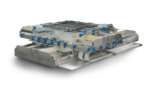
Image: Nanomotion Ltd.
Vacuum Compatibility
Roughly half of all semiconductor inspection tools operate in vacuum. SEM-based tools require pressures below 10^-4 Pa. Focused ion beam (FIB) tools need 10^-5 Pa or better. E-beam inspection tools operate at similar vacuum levels.
Piezoelectric actuators are inherently vacuum-compatible. The ceramic (PZT) is a sintered oxide with negligible vapor pressure. The electrodes are sputtered metal (typically nickel or silver). The primary outgassing sources are the adhesive layers used to bond the ceramic plates together and any organic materials in the actuator assembly (insulation, potting compound, lead wires).
Standard piezo stack actuators can be baked at 80 to 150 degrees Celsius (depending on the adhesive system) to reduce outgassing to acceptable levels. Outgassing rates below 10^-8 PaL/(scm^2) are readily achievable after a 24-hour bake at 120 degrees Celsius. For comparison, electromagnetic motors with organic insulation on their windings typically outgas at 10^-6 to 10^-5 PaL/(scm^2), even after baking.
Particle generation is another critical concern. Electromagnetic motors with bearings or sliding contacts are problematic in vacuum because wear particles contaminate the process chamber. Piezoelectric actuators with flexure-guided stages eliminate sliding contacts entirely, producing zero wear particles during operation. This is a decisive advantage for any tool where the stage operates near the wafer surface.
Magnetic Interference in Vacuum Tools
Electron beam and ion beam tools use magnetic or electrostatic lenses to focus the beam. Stray magnetic fields from electromagnetic motors can deflect the beam, directly degrading imaging resolution. A stray field of 1 microtesla at the beam column can deflect a 10 keV electron beam by several nanometers, which is unacceptable.
Piezoelectric actuators generate no magnetic field during operation. This eliminates a major source of interference and simplifies the electromagnetic compatibility design of the tool. When electromagnetic motors are used for the coarse stage (as they typically are), magnetic shielding and distance become critical design parameters. The fine piezo stage, being non-magnetic, adds no contribution to the stray field budget.
Throughput vs. Accuracy Tradeoffs
Inspection tools face a fundamental tension between throughput (wafers per hour) and measurement accuracy. Faster scanning means higher stage velocities and accelerations, which increase vibration, following error, and settling time. The motor selection directly affects where this tradeoff sits.
Scanning Speed
A typical wafer inspection scan covers a 300 mm wafer in a series of parallel stripes. For a SEM tool with a 1 micrometer field of view scanning at 100 MHz pixel rate, the stage moves at approximately 100 mm/s during image acquisition. At the end of each stripe, the stage must decelerate, step over by the stripe width, and accelerate back to scanning speed. The turnaround time directly reduces throughput.
The coarse stage handles the scanning motion. A linear motor can easily achieve 100 mm/s scanning speed with accelerations of 5 to 20 m/s^2 during turnarounds. The limiting factor for throughput is not the motor's force capability but the settling time: how quickly the stage reaches sub-nm stability after the turnaround transient.
Settling Time
Settling time to sub-nm levels is where piezo fine stages provide their greatest throughput advantage. After a step or turnaround, the coarse stage rings at its structural resonances (typically 50 to 200 Hz) with amplitudes of 10 to 100 nm. Without a fine stage, these vibrations must decay naturally, which takes 50 to 500 ms depending on damping.
A piezo fine stage with 1 kHz bandwidth can actively damp these oscillations, reducing settling time to 2 to 5 ms. For a tool performing 1000 turnarounds per wafer, reducing settling time from 100 ms to 5 ms saves 95 seconds per wafer. At a 30-wafer-per-hour throughput target, that 95 seconds represents an 80% increase in effective measurement time.
Step-and-Settle Operations
Some inspection modes use step-and-settle rather than continuous scanning. The stage moves to a measurement site, settles, acquires data, and moves to the next site. For a defect review tool visiting 1000 sites per wafer with 10 ms measurement time per site, the total measurement time is only 10 seconds. If the settle time per step is 50 ms, the total settle time is 50 seconds, dominating the wafer processing time.
Reducing settle time from 50 ms to 5 ms with a high-bandwidth piezo fine stage cuts the settle overhead from 50 seconds to 5 seconds, nearly tripling the tool's throughput for this operation mode.
Piezo Actuator Types for Wafer Stages
Several piezoelectric actuator configurations are used in wafer stage fine positioning.
Multilayer Piezo Stacks
The most common configuration. A multilayer stack consists of hundreds of thin (20 to 100 micrometer) PZT layers with interleaved electrodes, co-fired into a monolithic block. Typical dimensions range from 5 x 5 x 10 mm to 10 x 10 x 40 mm. A 40 mm stack produces approximately 40 micrometers of free stroke at 150 V, with a blocking force of 5 to 30 kN depending on cross-section.
For fine stage applications, three or more stacks are arranged in a kinematic flexure frame to provide multi-axis motion. A common arrangement uses three stacks per axis in a differential push-pull configuration, providing both positive and negative displacement from a central rest position.
Stack actuators offer the highest stiffness and force of any piezo configuration, with resonant frequencies of 10 to 50 kHz for the actuator alone. When coupled to a flexure stage with a 1 kg payload, the first resonant frequency typically drops to 500 Hz to 2 kHz, depending on the stage design.
Shear Actuators
Shear-mode piezo actuators deform laterally rather than longitudinally. They are less common in wafer stages but offer advantages for in-plane (X-Y) motion because they can produce lateral displacement without the need for a lever or flexure to convert longitudinal motion into lateral motion.
Shear actuators produce lower forces and displacements than equivalent stack actuators (typically 30% to 50% of the d33 performance) but achieve this in a more compact package for lateral motion applications.
Piezo Stepping Motors
For applications requiring long travel (millimeters to centimeters) with nanometer resolution, piezo stepping motors (also called stick-slip or inertial motors) provide an alternative to the coarse-fine architecture. These motors use a piezo actuator to move a slider in nanometer-scale steps, accumulating travel over many cycles.
However, piezo stepping motors sacrifice bandwidth for travel range. Their step rates (typically 1 to 20 kHz) limit scanning speed, and the stick-slip mechanism introduces positioning noise of 1 to 5 nm. For high-throughput 300 mm wafer stages, the coarse-fine architecture with a linear motor and piezo fine stage remains the preferred solution.
Feedback and Metrology Integration
A piezo fine stage is only as good as the metrology system that measures its position. The stage feedback loop requires a position sensor with resolution below 0.1 nm, bandwidth above 10 kHz, and range matching the fine stage travel (50 to 200 micrometers).
Capacitive Sensors
The most common sensor for piezo fine stages. Capacitive sensors measure the gap between a probe and a conductive target with resolutions of 0.01 to 0.1 nm over ranges of 10 to 200 micrometers. Their bandwidth is limited by electronics (typically 10 to 50 kHz) rather than the sensing principle. They are non-contact, non-magnetic, and vacuum-compatible.
A three-sensor configuration per axis provides redundant position measurement and enables in-situ calibration of sensor drift. For highest accuracy, differential sensing (measuring the gap on both sides of a target) cancels common-mode thermal drift and target surface roughness.
Laser Interferometers
For the coarse stage, laser interferometers provide absolute position measurement over the full 300+ mm travel range with sub-nm resolution. Modern heterodyne interferometers achieve 0.1 nm resolution at measurement rates of 10 MHz. The interferometer also measures the fine stage position (since the fine stage carries the interferometer mirror), providing an independent check on the capacitive sensor feedback.
In the highest-performance systems, the interferometer signal is used for coarse-fine handoff: the coarse stage servo drives to minimize the interferometer error, while the fine stage servo drives to minimize the capacitive sensor error. The two loops operate in nested fashion, with the fine stage loop running at 5 to 10x the bandwidth of the coarse stage loop.
Thermal Management
Piezoelectric actuators are efficient compared to electromagnetic motors, dissipating approximately 5% to 10% of the input electrical energy as heat during dynamic operation. For a fine stage driven at 100 Hz with 10 micrometer amplitude, the power dissipation is typically 0.1 to 1 W. This is far less than the 10 to 100 W dissipated by the coarse stage linear motors.
However, even 1 W of heat in a precision stage causes thermal gradients that distort the stage structure. The thermal behaviour of piezo motors under dynamic load must be understood and managed from the start of the stage design. A 1 degree Celsius temperature rise in an aluminum flexure stage causes approximately 23 nm of thermal expansion per centimeter of length. For a 100 mm stage, that is 230 nm of drift, far exceeding the sub-nm accuracy requirement.
Thermal management strategies include:
- Symmetric actuator placement: Arranging actuators symmetrically so that thermal expansion cancels at the point of interest.
- Invar or Zerodur stage bodies: Using low-CTE materials (Invar at 1.2 ppm/K, Zerodur at 0.05 ppm/K) for the stage body reduces thermal sensitivity by 10x to 500x compared to aluminum.
- Active cooling: Running temperature-controlled fluid through channels in the stage body to remove actuator heat. This adds complexity but is standard practice for high-throughput tools.
- Feedforward compensation: Measuring stage temperature and applying a correction to the position command based on a thermal model of the stage.
Wafer Chuck Design and Stage Dynamics
The wafer chuck is the interface between the wafer and the stage, and its design directly affects positioning performance. The chuck must hold the wafer flat (below 50 nm peak-to-valley over the exposure or measurement field), provide thermal control, and couple the wafer's inertia to the stage without introducing additional resonances.
Vacuum chuck flatness
Electrostatic or vacuum chucks pull the wafer flat against a reference surface. The chuck flatness specification (typically below 100 nm peak-to-valley) must account for:
- Chuck surface finish and polishing quality
- Particle contamination between chuck and wafer (a single 1 µm particle creates a 10 to 50 nm local wafer bow over a 5 mm radius)
- Thermal distortion from non-uniform chuck heating
- Chuck material stability over time (ceramics are preferred for long-term dimensional stability)
For SEM inspection tools, the chuck must also be electrically conductive to prevent charge buildup on the wafer backside. Silicon carbide (SiC) and alumina-doped ceramics provide the combination of flatness, electrical conductivity, and thermal stability these tools require.
Chuck flatness qualification is performed off-tool using laser interferometry or capacitive profilometry. A go/no-go test maps the chuck surface over a 300 mm field and flags any point exceeding the flatness budget. In production, chucks are re-qualified on a schedule tied to wafer count, because gradual contamination of the chuck surface is a primary source of in-field flatness degradation. Some advanced tools perform in-situ chuck flatness monitoring by measuring the wafer-to-chuck gap at multiple points before each exposure or scan, feeding corrections to the stage Z-axis to compensate for residual non-flatness.
Dynamic coupling between chuck and fine stage
The wafer chuck adds mass to the fine stage, lowering its first resonance frequency. A 300 mm wafer (125 g) plus chuck (200 to 500 g) adds 325 to 625 g to the moving mass. For a fine stage with 1 kg base mass and first resonance at 2 kHz, adding 500 g of chuck and wafer reduces the resonance to:
f_new = f_original × √(m_original / m_total) = 2000 × √(1.0 / 1.5) = 1633 Hz
This 18% reduction in resonance frequency reduces the achievable control bandwidth by a similar proportion, from perhaps 800 Hz to 650 Hz, which in turn reduces disturbance rejection by 4 dB at any given frequency.
Stage designers address this by:
- Minimizing chuck mass through topology optimization and material selection (SiC has excellent stiffness-to-weight ratio: E/ρ = 170 GPa / 3200 kg/m³)
- Using lightweight kinematic couplings between chuck and stage body to prevent over-constraining
- Tuning the controller for the loaded (wafer-present) condition, accepting slightly degraded performance during wafer exchange when the chuck is unloaded
The frequency shift from chuck loading is not just a design-time consideration. In tools that process multiple wafer sizes (150 mm, 200 mm, and 300 mm on the same platform), the moving mass changes by a factor of three or more across the product range. Stage controllers on multi-format tools must switch between pre-characterized gain sets when the wafer size changes. Piezo fine stages handle this well because their high actuator stiffness provides robust stability margins across a wide range of payload masses, whereas voice coil actuators with lower stiffness are more sensitive to mass changes and may require gain scheduling with tighter tolerances.
Chuck thermal management
The wafer process often generates heat (electron beam exposure, laser processing, high-intensity illumination). The chuck must absorb this heat and conduct it to the stage cooling system without creating thermal gradients that distort the wafer.
A typical thermal budget for a SEM inspection chuck:
- Beam power absorbed by wafer: 0.1 to 1 W (depending on beam current and dwell time)
- Allowable wafer temperature rise: < 0.1 °C (to prevent thermal drift exceeding 1 nm)
- Required thermal conductance from wafer to cooling: > 10 W/°C
This thermal conductance is achieved through:
- High-conductivity chuck material (SiC: 120 W/(m·K), AlN: 170 W/(m·K))
- Good thermal contact between wafer backside and chuck (helium backside gas cooling at 1 to 10 Torr, or direct mechanical contact for vacuum tools)
- Liquid cooling channels integrated into the chuck or the stage body beneath it
Worked Example: Fine Stage Bandwidth Requirement
Consider a 300 mm inspection tool with the following specifications:
- Coarse stage settling vibration: 50 nm peak at 100 Hz after a step move
- Required in-position stability: 0.5 nm peak-to-peak
- Disturbance rejection ratio needed: 50 nm / 0.5 nm = 100x (40 dB)
For a second-order control system (typical for a piezo fine stage), the disturbance rejection at frequency f is approximately (f_bw / f)^2, where f_bw is the closed-loop bandwidth.
To achieve 40 dB (100x) rejection at 100 Hz:
(f_bw / 100)^2 = 100
f_bw = 100 * sqrt(100) = 1000 Hz
So the fine stage needs a closed-loop bandwidth of 1 kHz to reject 100 Hz disturbances by 40 dB. This is a realistic but demanding specification. Achieving it requires a mechanical resonance frequency above 2 kHz (to provide adequate phase margin), which in turn requires a stiff flexure design with minimal payload mass.
If the disturbance frequency were 200 Hz instead of 100 Hz, the required bandwidth would double to 2 kHz, which pushes the mechanical resonance requirement above 4 kHz. This illustrates why minimizing coarse stage vibration frequencies (through structural design) is just as important as maximizing fine stage bandwidth.
Why Piezo Dominates This Space
The convergence of requirements for 300 mm wafer stage positioning, sub-nm resolution, zero magnetic interference, vacuum compatibility, zero particle generation, high bandwidth, and low heat dissipation, creates a specification space that only piezoelectric actuators can occupy.
Electromagnetic voice coil actuators could in principle achieve the resolution and bandwidth, but their magnetic fields, higher heat dissipation, and need for bearing or flexure guidance make them a poor fit for fine stages near charged particle beams. A detailed comparison of these technologies is available in the piezo versus voice coil article. For the vacuum motor selection decisions upstream of fine-stage design, see the companion article on vacuum-compatible motor selection.
MEMS actuators lack the force and travel range for 300 mm wafer stage payloads.
Magnetostrictive actuators share many of piezo's advantages but generate magnetic fields and have lower bandwidth due to eddy current losses.
Piezoelectric actuators are not perfect. Their hysteresis (10% to 15% for open-loop PZT stacks), creep (1% to 5% of displacement over logarithmic time), and limited travel range require careful engineering to manage. Understanding repeatability versus accuracy is essential here: the sensor closes the loop on accuracy, but the mechanical repeatability of the stage structure still sets a floor on what feedback can achieve. With closed-loop feedback from capacitive sensors, these limitations are rendered irrelevant: the sensor, not the actuator, determines the positioning accuracy. And for the combination of specifications that 300 mm wafer stage positioning demands, no other actuator technology comes close.
Edge Placement Error and Stage Contribution
At the 3 nm node and below, the semiconductor industry has shifted from traditional overlay and CD (critical dimension) specifications to a unified metric called edge placement error (EPE). EPE captures the total deviation of a pattern edge from its intended position, combining contributions from overlay, CD variation, and local pattern distortion. The stage positioning accuracy directly feeds into the EPE budget.
EPE budget allocation
A typical EPE budget at the 3 nm node is 2 to 3 nm (3-sigma). The contributors include:
| Contributor | Typical allocation (nm, 3-sigma) |
|---|---|
| Overlay (lithography) | 1.0 to 1.5 |
| CD uniformity | 0.5 to 1.0 |
| Local pattern placement (mask) | 0.3 to 0.5 |
| Metrology uncertainty | 0.3 to 0.5 |
| RSS total | ~2 to 3 |
For inspection and metrology tools, the stage positioning error contributes to the "metrology uncertainty" term. A 0.5 nm stage positioning error consumes the entire metrology allocation, leaving zero margin for sensor noise, algorithm error, or other measurement uncertainties. This is why the sub-nm stage positioning specification is not aspirational; it is mandatory.
How stage errors manifest in EPE measurements
When an inspection tool measures EPE, it must distinguish between actual pattern errors on the wafer and measurement artifacts caused by the tool itself. Stage positioning errors create measurement artifacts that appear as:
- Systematic offsets: if the stage has a repeatable position error at a specific wafer location, the EPE measurement at that location is biased. This bias cancels only if the measurement is repeated with the wafer rotated, which doubles measurement time.
- Random scatter: stage repeatability errors add noise to EPE measurements. For N repeated measurements at the same location, the stage contribution to measurement noise is reduced by √N, but at the cost of N× measurement time.
- Field-dependent errors: if the stage has position-dependent accuracy errors (e.g., from encoder interpolation), EPE measurements show systematic field-dependent patterns that can be confused with real lithography errors.
Calibration strategy for EPE-capable tools
To support EPE measurements at the 3 nm node, inspection tools implement multi-layer calibration:
-
Geometric calibration: laser interferometer mapping of stage XY accuracy, performed daily or weekly. Residual error after calibration must be below 0.3 nm across the measurement field.
-
Dynamic calibration: measurement of stage following error during scanning at operational velocities. The following error profile is stored and subtracted from measurement data in post-processing.
-
Thermal calibration: characterization of stage drift versus internal temperature sensors. The thermal model predicts position drift to within 0.1 nm per 0.01 °C change.
-
Cross-calibration: periodic comparison of EPE measurements against a reference metrology tool (typically a CD-SEM or atomic force microscope operating at lower throughput but higher accuracy). Discrepancies exceeding 0.5 nm trigger recalibration.
The piezo fine stage's sub-nm repeatability is what makes this calibration strategy feasible. A stage with 5 nm repeatability would require prohibitively long averaging to achieve the same measurement uncertainty, reducing tool throughput below economically viable levels.
Beyond throughput, there is an important statistical consideration. EPE at advanced nodes is characterized not just by its mean value but by its tail distribution: the 99th-percentile EPE that drives yield loss. A stage with poor repeatability inflates the apparent tail of the EPE distribution, making it impossible to distinguish real process outliers from measurement noise. This ambiguity forces engineers to either widen process windows (accepting lower yield) or increase measurement sampling (accepting lower throughput). A piezo fine stage with sub-nm repeatability keeps the measurement noise floor well below the process variation being characterized, preserving both yield and throughput. It is in this sense that the stage positioning specification is a system-level requirement: it defines not just what the tool can measure, but what the process engineer can actually know.